

How to reduce RF effects in PCB interconnect design? Keep these tips in mind
Article source:PCBworld Dated :2023/02-12
Introduction: This article will introduce various techniques for the design of three types of interconnects in circuit board systems: chip to circuit board, intra PCB interconnects, and between PCBs and external devices, including device installation, wiring isolation, and measures to reduce lead inductance, to help designers reduce the RF effect in PCB interconnect design.
The interconnection of circuit board systems includes three types of interconnections: chip to circuit board, intra PCB interconnections, and between PCBs and external devices. In RF design, the electromagnetic characteristics at interconnect points are one of the main issues faced in engineering design. This article introduces various techniques for the above three types of interconnect design, including device installation methods, wiring isolation, and measures to reduce lead inductance.
There are currently indications that printed circuit board designs are becoming increasingly frequent. With the continuous growth of data rates, the bandwidth required for data transmission also drives the signal frequency limit to 1 GHz or even higher. Although this high-frequency signal technology is far beyond the range of millimeter wave technology (30 GHz), it does also involve RF and low-end microwave technology.
RF engineering design methods must be able to handle the strong electromagnetic field effects that typically occur at higher frequencies. These electromagnetic fields can induce signals on adjacent signal lines or PCB lines, causing annoying crosstalk (interference and total noise), and can damage system performance. Backloss is mainly caused by impedance mismatch, which has the same impact on the signal as additive noise and interference.
High return losses have two negative effects:
1. Signal reflection back to the signal source will increase system noise, making it more difficult for the receiver to distinguish between noise and signal;
Any reflected signal will essentially degrade the signal quality due to changes in the shape of the input signal.
Although digital systems only process 1 and 0 signals and have very good fault tolerance, the harmonics generated when high-speed pulses rise can lead to weaker signals with higher frequencies. Although forward error correction technology can eliminate some negative effects, part of the system's bandwidth is used to transmit redundant data, resulting in reduced system performance. A better solution is to let the RF effect contribute to, rather than undermine, the integrity of the signal. It is recommended that the total return loss at the frequency of the digital system (typically at poor data points) be - 25 dB, equivalent to a VSWR of 1.1
The goal of PCB design is to be smaller, faster, and cheaper. For RFPCBs, high-speed signals sometimes limit the miniaturization of PCB designs. Currently, the main methods to solve the crosstalk problem are to conduct ground layer management, spacing between wires, and reducing lead inductance. The main method of reducing return loss is impedance matching. This method includes effective management of insulating materials and isolation of active signal lines and ground wires, especially when there is a state jump between the signal line and ground.
Due to the fact that interconnection points are the weakest link in the circuit chain, in RF design, the electromagnetic properties at the interconnection points are the main problem faced by engineering design. It is necessary to investigate each interconnection point and solve the existing problems. The interconnection of circuit board systems includes three types of interconnections: chip to circuit board, intra PCB interconnections, and signal input/output between PCBs and external devices.
1、 Interconnection between chips and PCB boards
Pentium IV and high-speed chips containing a large number of input/output interconnection points have been introduced. As far as the chip itself is concerned, its performance is reliable, and its processing rate has been able to reach 1GHz. At the near GHz interconnection seminar, the exciting thing is that the methods for dealing with the growing number and frequency of I/Os have become widely known. The main problem with interconnection between chips and PCBs is that too high interconnection density can lead to the basic structure of PCB materials becoming a factor limiting the growth of interconnection density. An innovative solution was proposed at the conference, which uses a local wireless transmitter inside the chip to transmit data to adjacent circuit boards. Regardless of whether this scheme is effective or not, participants are very clear that in terms of high-frequency applications, IC design technology has far surpassed PCB design technology.
2、 PCB board interconnection
The techniques and methods for designing high-frequency PCB are as follows:
A 45 ° angle should be adopted at the corner of the transmission line to reduce return loss (Figure 1);
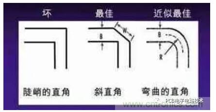
Figure 1: Tips for high-frequency PCB design: using a 45 ° angle for transmission corners
2. High performance insulated circuit boards with strictly controlled insulation constants and levels should be used. This method is conducive to effective management of the electromagnetic field between the insulating material and adjacent wiring.
3. Improve PCB design specifications for high-precision etching. Consider specifying a total line width error of+/-0.0007 inches, managing the undercut and cross section of wiring shapes, and specifying wiring sidewall plating conditions. Overall management of wiring (wire) geometry and coating surfaces is important to address the skin effect issues associated with microwave frequencies and to achieve these specifications.
4. There is a tap inductance in the protruding lead, so avoid using components with leads. Use surface mount components in high-frequency environments.
5. For signal vias, it is important to avoid using a through hole machining (pth) process on sensitive boards, as this process can cause lead inductance to be generated at the vias. When a through hole on a 20 layer board is used to connect layers 1 to 3, the lead inductance can affect layers 4 to 19.
6. Abundant ground planes shall be provided. Molded holes should be used to connect these ground planes to prevent the impact of 3-dimensional electromagnetic fields on the circuit board.
"To choose a non electrolytic nickel plating or gold immersion plating process, do not use the HASL method for electroplating.". This plated surface can provide better skin effect for high-frequency currents (Figure 2). In addition, this highly solderable coating requires fewer leads, helping to reduce environmental pollution.
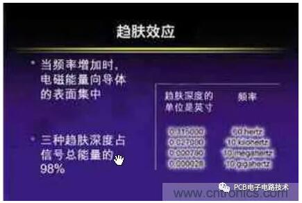
Figure 2: Tips for high-frequency PCB design: skin effect
The solder resist layer prevents the flow of solder paste. However, due to thickness uncertainty and unknown insulation properties, covering the entire plate surface with solder resist materials will lead to significant changes in electromagnetic energy in microstrip design. Generally, solderdam is used as the welding resistance layer.
If you are not familiar with these methods, you can consult with an experienced design engineer who has worked in military microwave circuit board design. You can also discuss with them the price range you can afford. For example, using a copper clad coplanar microstrip design is more economical than a stripline design, and you can discuss this with them to obtain better suggestions. 's engineers may not be accustomed to considering cost issues, but their recommendations can also be quite helpful. It will be a long-term job to train young engineers who are unfamiliar with RF effects and lack experience in handling them.
In addition, other solutions can be adopted, such as improving the computer model to provide RF effect processing capabilities.
3、 PCB is interconnected with external devices
It can now be considered that we have solved all signal management issues on the board and on the interconnections of various discrete components. So how to solve the signal input/output problem from the circuit board to the wire connecting the remote device? Trompeter Electronics, the innovator of coaxial cable technology, is working to solve this problem and has made some important progress (Figure 3). In addition, take a look at the electromagnetic field shown in Figure 4 below. In this case, we manage the transition from microstrip to coaxial cable. In coaxial cables, the ground wire layers are annular interleaved and evenly spaced. In microstrip, the ground plane is below the active line. This introduces certain edge effects that need to be understood, predicted, and considered during design. Of course, this mismatch can also lead to back loss, and it must be reduced to avoid generating noise and signal interference.
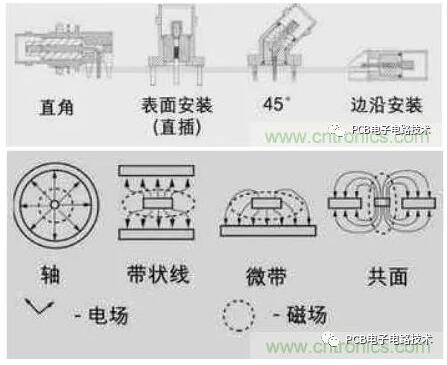
Figure 3 and Figure 4: PCB and External Device Interconnection Techniques
The management of impedance issues within a circuit board is not a negligible design issue. The impedance starts at the surface of the circuit board and ends at the coaxial cable through a solder joint to the connector. As impedance varies with frequency, the higher the frequency, the more difficult impedance management becomes. The problem of using higher frequencies to transmit signals over broadband appears to be a major issue in design.
Factory address: Mintai Industrial Park, Guantang Road, Huangjiang Town, Dongguan City, Guangdong Province
Office Address: Room 801, Dongtang Yongdongxing Building, Shajing Street, Bao'an District, Shenzhen
86-0755-33134847
86-0755-29868282


