

All the BGA welding issues you want to know are here
Article source:PCBworld Dated :2023/03-27
BGA is a type of chip packaging, short for Ball Grid Array. The packaging pins are spherical grid arrays at the bottom of the package. The pins are all spherical and arranged in a pattern similar to a grid, hence the name BGA.
Many motherboard control chips use this packaging technology. Memory packaged using BGA technology can increase its capacity by 2-3 times without changing its size. Compared to TSOP, BGA has smaller size, better heat dissipation, and electrical performance.
BGA Packaging Pad Routing Design
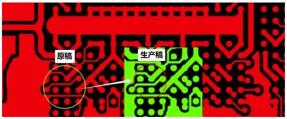
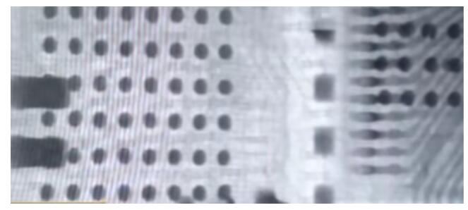
BGA pad to pad routing
During design, when the spacing between BGA pads is less than 10 mil, no wiring is allowed between two BGA pads, as the line width spacing exceeds the production process capacity. Unless the BGA pads are reduced, ensure that their spacing is sufficient when making production drafts. However, when the pads are cut into abnormal shapes, it may lead to inaccurate welding positions.
Resin plug hole electroplating and leveling in disk
When the bonding pad spacing for BGA packaging is small and it is not possible to wire out, it is necessary to design a hole in the pad, punch the hole on the pad, and route the wire from the inner layer or the bottom layer. At this time, the hole in the pad needs to be filled with resin plug hole electroplating. If the resin plug hole process is not adopted for the hole in the pad, poor welding will occur due to the small welding area of the hole in the middle of the pad, and tin leakage will also occur in the hole.
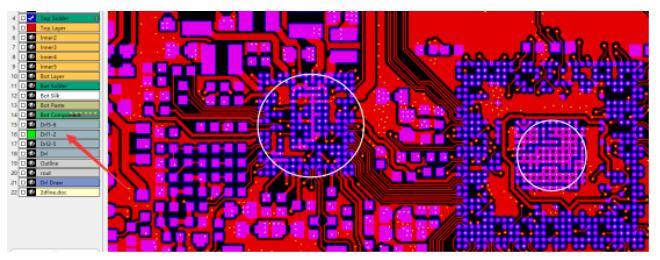
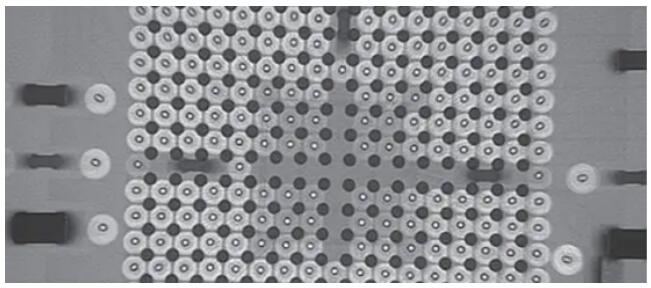
BGA area via plug hole
The vias in the BGA pad area generally require plug holes. Considering the cost and ease of production of the template, the basic vias are covered with oil. The ink plug hole is selected as the plug hole method. The advantage of the plug hole is to prevent foreign matters in the hole or protect the service life of the vias. Moreover, during reflow soldering of the SMT patch, tin from the vias can cause a short circuit on the other side.
Hole in disk, HDI design
For BGA chips with small pin spacing, it is recommended to directly design the hole in the board when the pin pad cannot be made out beyond the process. For example, if the BGA chip on the mobile phone board is relatively small and has many pins, and the pin spacing is too small to be routed from the middle of the pins, the HDI blind buried hole wiring method can only be used to design the PCB. Drill the hole in the board above the BGA pad, drill the buried hole in the inner layer, and conduct the wiring in the inner layer.
BGA welding process
Printing tin height
The purpose of solder paste printing is to evenly apply an appropriate amount of solder paste to the PCB pads to ensure good electrical connection and sufficient mechanical strength when reflow soldering the pads corresponding to the chip components and the PCB. The printing of solder paste requires the production of a steel mesh. The solder paste passes through the corresponding openings in the steel mesh of each pad, and under the action of a scraper, evenly coat the tin on each pad to achieve good soldering.
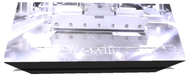
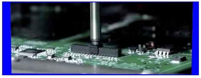
Device placement
Device placement refers to the placement of a chip. Using a mounting machine, you can accurately mount a chip component to the corresponding position on the surface of the PCB that has been printed with solder paste or mounting adhesive. High speed mounting machines are suitable for mounting a large number of small components, such as capacitors, resistors, etc., as well as some IC components; Universal mounting machine, suitable for mounting components with high specificity or precision, such as QFP, BGA, SOT, SOP, PLCC, etc.
Reflow soldering
Reflow soldering is the mechanical and electrical connection between the solder ends of surface mounted components and the PCB pad by melting the solder paste on the circuit board pad, forming an electrical circuit. Reflow soldering is a key process in SMT production. Reasonable temperature curve settings are key to ensuring the quality of reflow soldering. Improper temperature curves can cause solder defects such as incomplete soldering, faulty soldering, component warping, and excessive solder balls on the PCB board, affecting product quality.

X-Ray inspection
X-Ray can inspect almost all process defects. Through its perspective characteristics, it can check the shape of solder joints and compare them with the standard shapes in the computer library to determine the quality of solder joints. Especially for BGA and DCA components, the function of solder joint inspection is irreplaceable, and there is no need to test molds. The disadvantage is that the price is currently quite expensive.
Reasons for poor BGA welding
BGA pad hole not processed
There are holes in the bonding pad for BGA welding, and the solder balls will be lost together with the solder during the welding process. Due to the lack of resistance welding process in PCB production, solder and solder balls will be lost through the holes close to the solder board, resulting in solder ball loss.
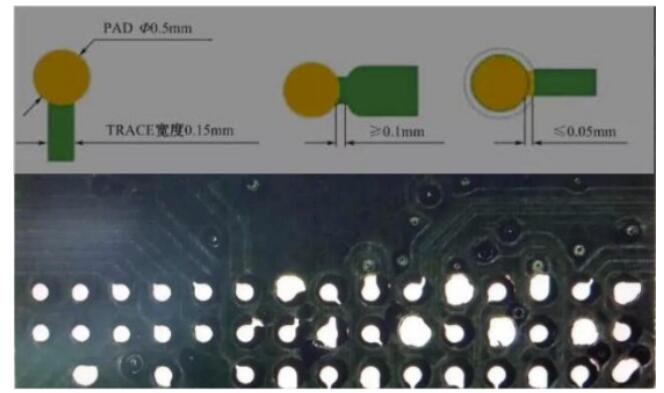
Different pad sizes
The size of the BGA welding pad varies, which can affect the quality and yield of the welding. The outgoing line of the BGA welding pad should not exceed 50% of the pad diameter, and the outgoing line of the power welding pad should not be less than 0.1mm, and can be thickened. To prevent the deformation of the welding pad, the welding barrier window should not be greater than 0.05mm. The window on the copper surface should be as large as the line PAD, otherwise, the size of the BGA welding pad made is different.
Quickly solve BGA welding problems
It is not uncommon for related problems to arise during production due to improper preliminary design. What are some ways to solve production problems once and for all and in advance? I have to mention a software that can perfectly avoid production risks: Huaqiu DFM.
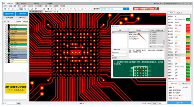
Encapsulated disk hole
Use the DFM one-click analysis function to detect whether there are holes in the design file, and prompt the design engineer whether there are holes in the disk that need to be modified in the file. Because the manufacturing cost of the holes in the disk is very high, if the holes in the disk can be changed to ordinary holes, it can reduce the cost of the product. At the same time, it also reminds the manufacturing board factory that there are holes in the disk that need to be designed, and it is necessary to do resin plug holes to go through the production process of the holes in the disk.
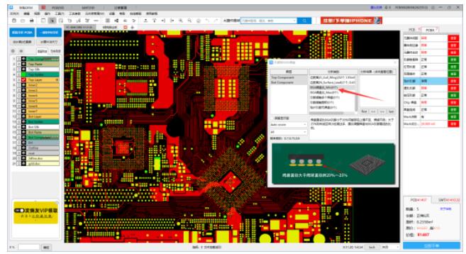
Pad to pin ratio
Use the DFM assembly analysis function to detect the size ratio of the BGA pads in the design file to the actual device pins. If the pad diameter is less than 20% of the BGA pin, there may be a poor soldering problem. If it is greater than 25%, the wiring space will be reduced. At this time, the design engineer needs to adjust the ratio of the pad diameter to the BGA pin diameter.
DFM software provides detailed solderability solutions for issues such as BGA pads. It helps users review the solderability of BGA design documents before production, avoids solderability issues with BGA chips during assembly, and prompts BGA chips for solderability quality issues.
Currently, a new version of DFM software has been released, which can synchronize the manufacturing and design processes, simulating the entire production process of selected PCB products from design, manufacturing, to assembly.
DFM connects the four modules of BOM sorting, component matching, bare board analysis, and assembly analysis to work together to complete a complete DFM analysis!
Factory address: Mintai Industrial Park, Guantang Road, Huangjiang Town, Dongguan City, Guangdong Province
Office Address: Room 801, Dongtang Yongdongxing Building, Shajing Street, Bao'an District, Shenzhen
86-0755-33134847
86-0755-29868282


